Prelude
This post is meant to demonstrate my general workflow of how I create a VHDL model of a chip from its datasheet. I’ll skip over how to analyze and run simulations in VHDL. This will be the subject in the next post where I present a build system/project structure I found on Github and how I modified it to work with the VHDL-2008 standard. Here’s a quick overview how that process works.
Then I’ll show you the steps I take to combine the VHDL models of memory and logic chips into self-contained modules that I will use in the Wasp. Specifically, I will model the RAM chip, an 8-bit data, and an 11-bit address output module. These will represent the LED outputs on the Wasp’s front panel.
WARNING: As of the writing of this post (February 2019), it is my understanding that Xilinx Vivado does not support unconstrained arrays yet as defined in the VHDL-2008 standard. I will use unconstrained arrays in my code examples. My code is tested with ghdl only. So it may need adjustments to run with other VHDL suits and/or simulators.
Choosing the RAM
Since the Wasp is a ROMless design, accessing the RAM via the toggle switch interface must be rock-solid. But before I can access RAM, I need to choose a RAM chip that is practical.
Assuming an 8-bit processor as CPU in the Wasp, it is safe to say that the Wasp will be able to address up to 64 KB at most. While there are some 8-bit processors like later Z80 models that have a 24-bit address bus, the vast majority of 8-bit processors had a 16-bit address bus and could, therefore, address up to 64 KB of memory.
Since the Wasp will be a ROMless design and will lack any fancy interfaces to the outside, the memory map for this system will be very simple.

Now the question is, how much RAM is necessary or enough for the Wasp? I could go for the full 64 KB. But that doesn’t seem like a good idea for two reasons. One, since the user will only be able to “toggle in” code by hand, it is safe to assume that no one would write and run programs of several kilobytes on the Wasp. Two, should I at a later point decide that I do want to add additional functionality or interfaces, I’d need to throw away the memory map and parts of the glue logic.
So, I’m not going to use the full 64 KB. Then the decision comes down to another factor, availability. Online shops like Mouser or Farnell offer good (some would consider that debatable) search tools for filtering chips to certain specs. After some searching and checking, I settled for the 6116SA/LA. It’s a 2K x 8-bit SRAM chip that is available in multiple packages (DIP and SOIC) and carried by multiple shops for a reasonable price range.
Modeling RAM in VHDL
Implementing the 6116SA/LA is straight forward. You’ll find a lot of examples on how to implement memory chips in VHDL online. So I’ll just skim quickly over my code.
The 6116 has three control signals:
- CS: Chip Select
- WE: Write Enable
- OE: Output Enable
All signals are active-low as evident by the bar over the signal name. Then there is an 11-bit address bus and an 8-bit data bus. That’s all there is to the 6116 RAM chip. The exact function of the control signals can be seen in the Truth Table on page 2 of the datasheet:
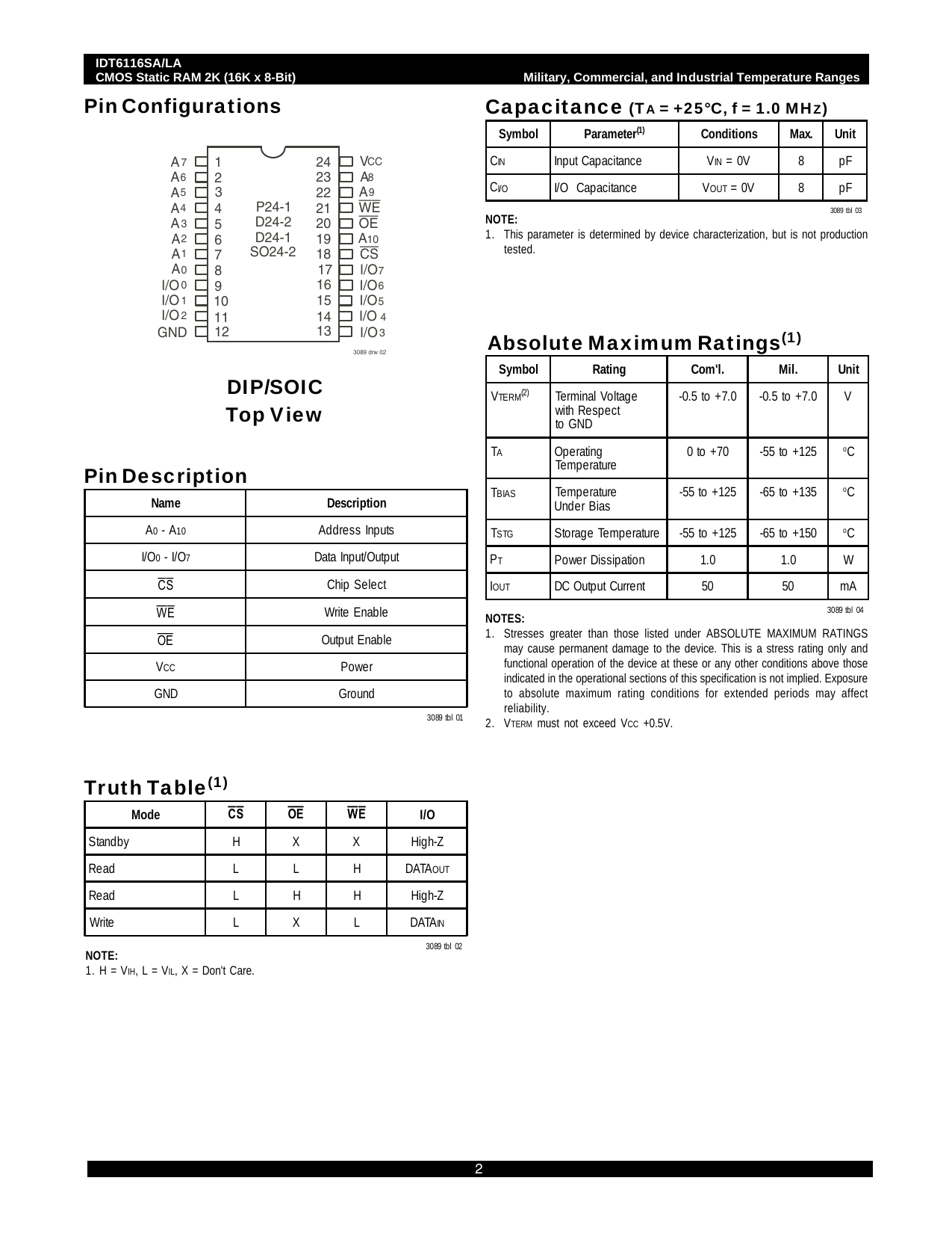
So there is no real surprise here in how this RAM chip operates. So let’s see how this translates into VHDL code:
There’s not a lot to discover here. I define the 6116 RAM chip as an entity with an interface (port in VHDL lingo) made of the three control signals and two buses mentioned above. I use generics for simplicity. If at a later stage I’d decide to use a larger RAM chip, I’d simply increase ADDR_WIDTH. The subsequent implementations in the entity’s architecture would adjust accordingly. Extending the data bus to say 16-bit (some modern chips use 16-bit data buses) can be achieved in the same manner.
If you’re completely new to VHDL, you might be wondering about the std_logic type. This type is similar to boolean types in other languages like C++. But unlike bool in C++, std_logic can hold a total of 9, not only 2 states:
-
U: uninitialized. This signal hasn’t been set yet. -
X: unknown. Impossible to determine this value/result. -
0: logic 0 -
1: logic 1 -
Z: High Impedance -
W: Weak signal, can’t tell if it should be 0 or 1. -
L: Weak signal that should probably go to 0 -
H: Weak signal that should probably go to 1 -
-: Don’t care.
This throws off a lot of people when they switch from a programming language to an HDL. And this is because, say it with me, VHDL is not programming. We’re simulating digital circuits here. For example, when designing and testing a circuit it can be useful to differentiate between a logic 1 coming from a chip’s output pin driving an input pin of another chip; and an input pin simply being “driven” by a pull-up resistor, represented here by the H state. Or when designing and optimizing glue logic circuits you may have used a Karnaugh-Veitch-Map to reduce complexity; std_logic can help there since it has the don’t care state - too.
Well, I said this was not going to be a VHDL tutorial, so back to the code itself.
There are two processes in this architecture, one for reading, one for writing memory. Both come with a sensitivity list. This means whenever one of the signals mentioned in the sensitivity list changes value (low to high, high to low, low to high-impedance, etc.), then the process is invoked. The process then checks if the control signals and reads or writes to/from memory accordingly.
I haven’t implemented the metastability check process yet for the RAM chip because I want to devote its own blog post to this topic at a later date.
Next, we need a way to verify that our VHDL model works properly. This is done with a so-called test bench. A test bench in it’s most simple form is an entity with an empty port that instantiates the device under test (dut) and generates some test signals. Here’s a simple test bench I’m going to expand later:
This test bench will generate the timing diagram shown in the first blog post:
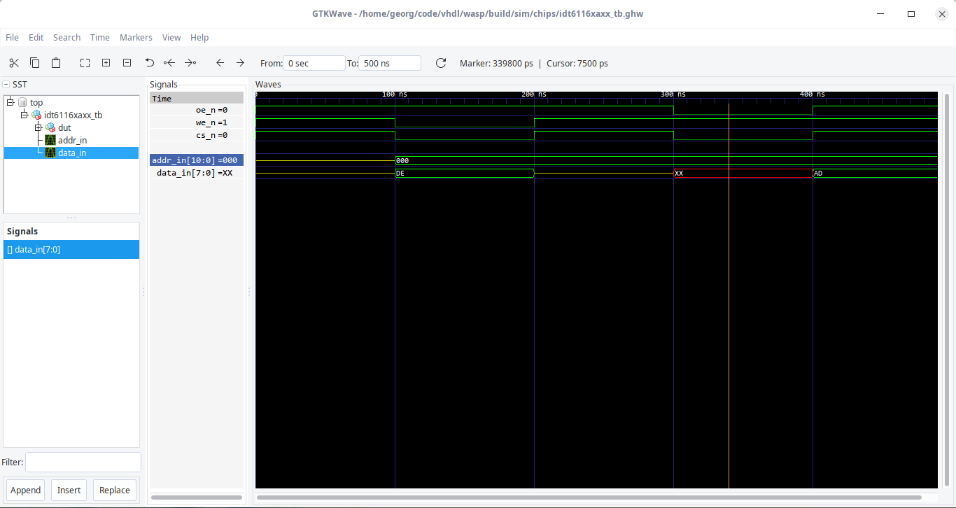
While this is not a very thorough test of the RAM chip model, it’s sufficient for now. I still have to implement the metastability check process. Later, when I test the simple output module.
A Simple Output Module
Next, I want to design a simple, self-contained module that has this interface:
- A Latch signal that will tell the module to latch new input data into the module
- An 8-bit input bus for the data that will be shown in the front panels LEDs
- An 8-bit output bus to drive the front panel data LEDs
Simple as that. Here’s a simple sketch:
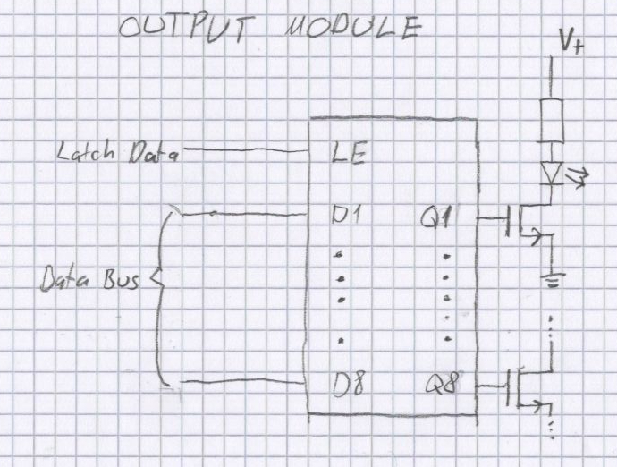
Thankfully, there’s a chip that does almost exactly that. The SN74AHC573 Octal Transparent D-Type Latches With 3-State Outputs is the ideal candidate for this. As I said, I’m a minimalist. So I’m not going to reinvent the wheel here. So let’s look at the code:
Again, not a lot of surprises here. I add a few constants that represent the timing characteristics. They’re lifted straight from the datasheet on page 6. I latch the input first into an internal signal for two reasons. One, it’s common and good practice in VHDL to map input signals to an internal one, modify or react to it, then simply update the output signal(s) accordingly. Two, the SN74AHC573 can latch new data even while the output is disabled (OE is high). I’m not using this feature right now but I might in the future.
Next, a simple test bench:
Unlike the RAM test bench above, this test bench also checks for metastability violations.
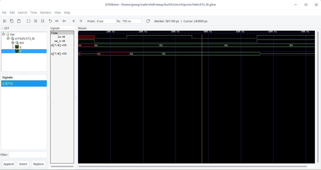
If I uncomment the metastability violations and run the simulation again, ghdl will complain:
$ ./sim/chips/sn74ahc573_tb
/home/wasp/src/chips/sn74ahc573.vhdl:68:9:@751500ps:(assertion warning): Input signal changed during hold time!
/home/wasp/src/chips/sn74ahc573.vhdl:55:9:@755ns:(assertion warning): LE pulse width too short!
/home/wasp/src/chips/sn74ahc573.vhdl:61:9:@771ns:(assertion warning): Input changed during setup time!
/home/wasp/src/chips/sn74ahc573.vhdl:68:9:@772500ps:(assertion warning): Input signal changed during hold time!
Since this is the only digital component, I can finally design my data output module:
As you can see, it’s basically just the 74AHC573 with the OE pin tied to ground. Okay, but why write an extra model for the output module if it’s basically the same as the chip model itself? One, it’s more elegant since I only have to concern myself with the latch signal and can ignore the OE signal; this reduces the number of signals (and therefore complexity) in the long run. Two, I can pretty much copy-paste the code for the address output module. Since I’m using a 2K x 8-bit RAM, I need an 11-bit module to indicate the current address on display. Here’s the code for the 11-bit address output module:
See how easy it is to design a new module this way? I simply add a second SN74AHC573 chip to handle the address bits 8 through 10, and tie the unused pins to ground.
There’s a lot of code repetition between the data and address module. There are ways to generalize this. I’ll do so in a later post with the help of type records. For now, let’s keep it this way for simplicity.
Okay, we have RAM and modules for displaying data and address. Let’s put it all together into a simple first version of the Wasp.
A Simple first Wasp
Here are the system’s parts (check the sketch at the end of this post):
- The IDT6116SA RAM chip
- An 8-bit output module connected the data bus that will display the data last read from RAM
- An 11-bit output module connected to the address bus that will display the address last selected
- A simple front panel with two buttons, “Write Data” and “Read Data”; this includes a bit of simple glue logic to generate the appropriate control signals
- For simplicity, I’m keeping the data and address input separated for now
That’s all there is to it. I will drive the data and address buses “by hand” for now. Here’s the code:
There’s one instance of each VHDL model I wrote earlier. Additionally, I add some “glue logic” to generate the correct control signals for the RAM and output modules. Now, let’s give the simple Wasp some input with, of course, another test bench:
And here is the timing diagram generated by it:
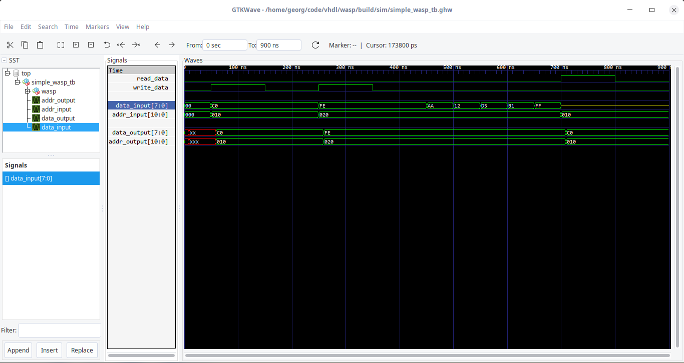
Mind, this is not a very thorough test of the functionality. But since the design is not really complex, there is no real value in writing a more robust test bench yet. Finally, here’s a sketch of the Wasp so far:

It’s a very simple system so far. But this sketch and the simulation result already show some problems that will need fixing. For example, there has to be a way to decouple the input switches from the data and address buses while data is read from the RAM, else this might result in a bus conflict. In fact, in the simulation code above I cheat a bit by setting the input bus to high-impedance “manually” before reading from RAM (check line 82).
Also, while I used separate signals for the data and address latch signals in the VHDL simulation, I simplify it in this sketch to one OR-gate. These are just two of the things I learned from the simulation and simply sketch. There’s a few other issues but I hope this demonstrates a bit how VHDL simulations can help find flaws in your design before hardware prototyping.
Conclusion
This turned out a bit longer than I planned. But I wanted to show my general workflow from component selection, schematic sketching, extracting vital pieces of information from datasheets, writing a VHDL model and its test bench. I skimmed over a lot of stuff, but I plan future posts to be a bit more granular.
[Next time][19], I’ll show you how I organize my project files and run simulations with the help of cmake.