Prelude
In the second post of this series, I designed simple models for representing three parts of the Wasp: RAM, data output, and address output. Then put them together in a first simple model of the Wasp.
Next, I’ll try to improve the simple Wasp design by adding the ability to read out memory with an Examine switch. When it is pressed/actuated, the Wasp will look up the datum at the address toggled in on the front panel, and display it on the output module. It serves the same function as the read_data signal (see sketch below) in the simple Wasp design.
My general approach will be one of black boxing: I’ll define input and output signals for each module. After that, I’ll work my way back from the signals to design the modules itself.
This will yield three new modules I will design and implement over the course of the next few posts.
Generating Control Signals
Let’s recall what I’ve got so far:
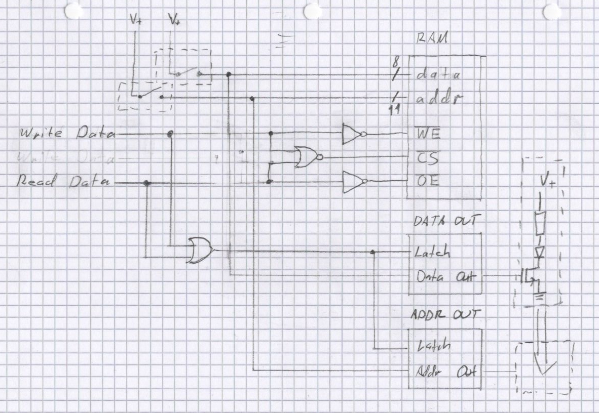
I want to expand this design to do the following:
- Allow for the user to examine the datum at any address in RAM
- Decouple the input from the address bus in a way that avoids bus conflicts then another part (namely, the CPU) is driving the address bus
- Generate the correct control signals for all chips and modules from the user’s input
To this end, I’ve updated the Wasp’s design like this:
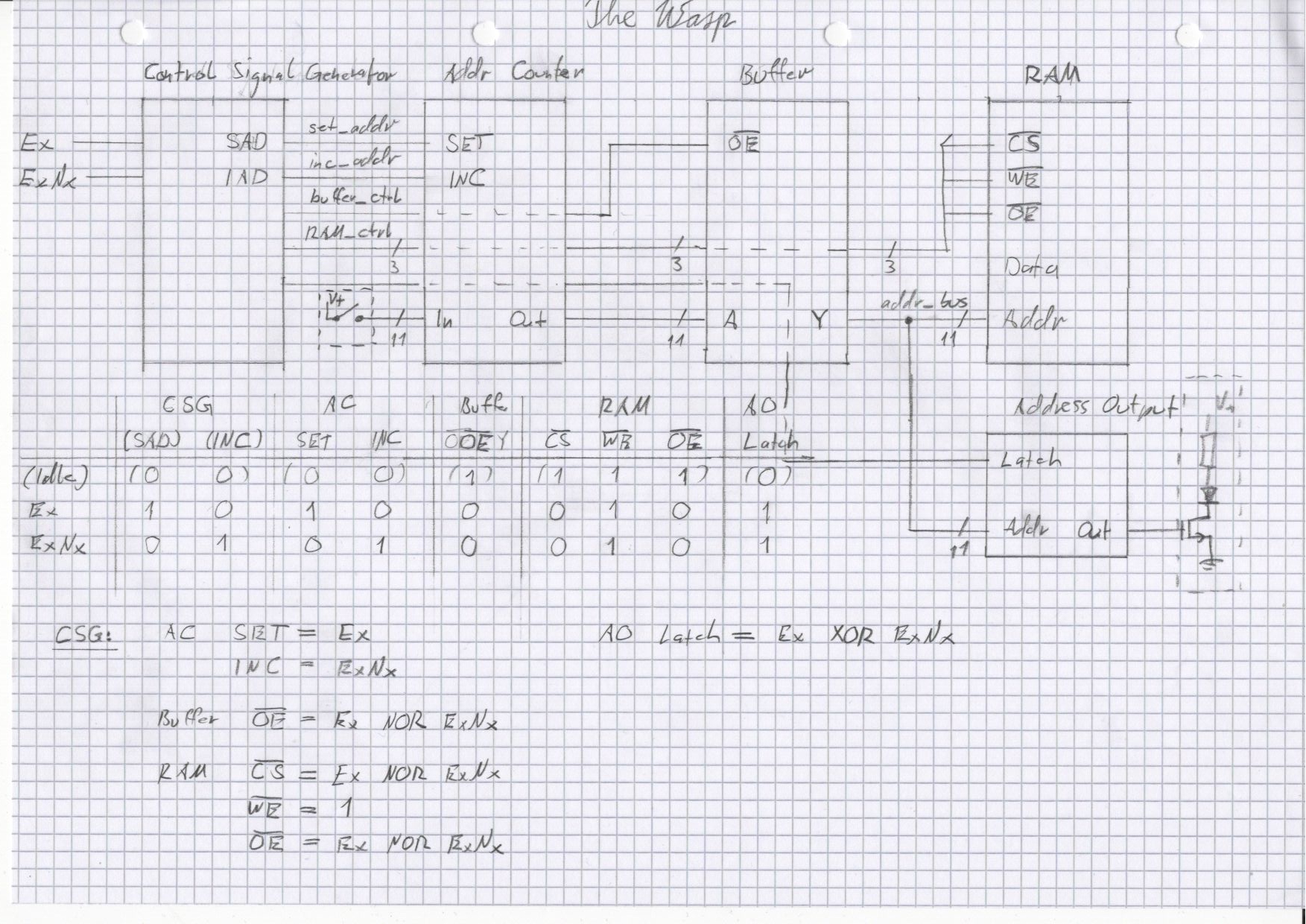
Let’s go through this part by part.
On the right-hand side, you can see the RAM and address output module. You know them already from last time. So, nothing new here. Please note, that I skipped the data output module for clarity. It is still there and will show up later again.
Now let’s jump to the left-hand side. On the very left edge of the system sketch, you can see two signals called Ex and ExNx - these represent the Examine and Examine Next switches. They both enter into a new module of the Wasp called the Control Signal Generator.
To the right of the CSG is the Address Counter. The Address Counter has two control signals:
- SET: Will latch the current state from the input switches (shown in the small box between CSG and Adress Counter) into the Address Counter
- INC: Will increment the address currently held in the Address Counter by one.
This pretty much mirrors the Examine and Examine Next switches’ functions.
Finally, there’s the Buffer. This will simply be a chip that will decouple the address bus from the address input to prevent bus conflicts. It has only one control signal, /OE. When /OE is low, the buffer’s output will drive the address bus, else the buffer’s output will be in high-impedance state.
In the lower half of the system sketch, I created a simple truth table. It has three rows, each representing a function.
First, there’s the Idle state. Idle is not really a function, but the state the system is in when there is no input to react to. These are the values each control signal should default to in case there is no (valid) input.
In the second row are the control signal values for Examine. The user wants to read data from a certain memory location.
In the last row are the control signal values for Examine Next.
To help you understand better what is happening here, let’s follow the Examine signal through the system. First, we need to latch the address to examine into the address counter. So we put the set_addr line in a high state to tell the Address Counter to latch the input switches. The Address Counter will latch the input and put it onto its OUT pins.
Next, the address emitted by the Address Counter goes into the Buffer. Since we’re trying to read from memory, the buffer has to let the address signal “pass” onto the address bus, so OE has to be in low state.
Finally, the RAM’s control signals have to be set correctly so the RAM will but the data found at the given address on the data bus (not represented on the system sketch). Also, the new address (and data) should be shown to the user, so the latch signal of the address output module is put in a high state too.
Implementing the Control Signal Generator
Let’s implement a first simple version of the Control Signal Generator. Here’s the truth table from the system sketch above with the signal composition:
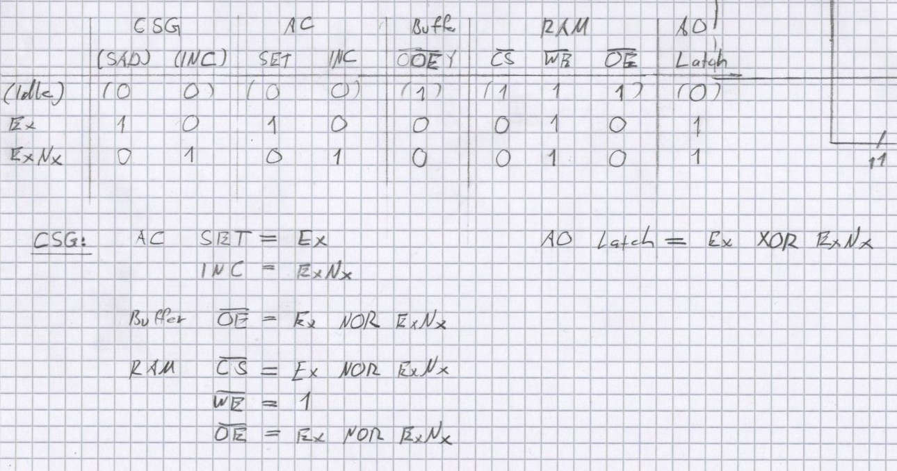
I simply derived the control signals from the truth table. Right now, the signal generator is pretty simple. But as I add functionality, its complexity will rise. So I’m not going to model the Control Signal Generator with existing chips yet. Here’s the VHDL code followed by its test bench:
No big surprises here. I translate the truth table above into signal assignments with simple NOR and XOR gates. But to make it behave a bit realistically, I add a propagation delay of 15 ns to each signal. This is a good average value for logic chips of the AC and AHC family. Here’s the simulation result:
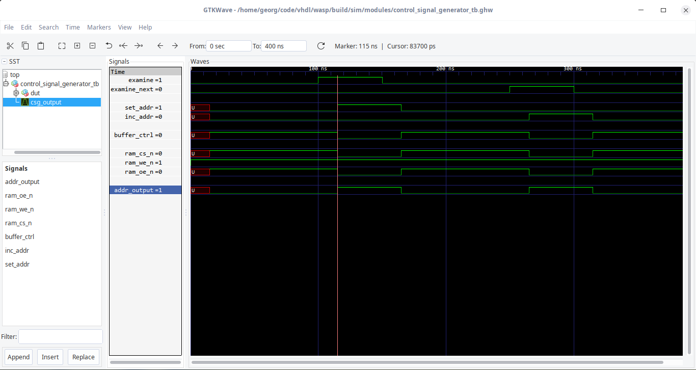
Again, this is a very simple model. This module will change various times over the course of the development. So this simplified approach should be sufficient for now. Next, let’s do a simple buffer.
Implementing a Buffer
The Buffer is even easier in terms of signal complexity:
And here is the result of the test bench above:
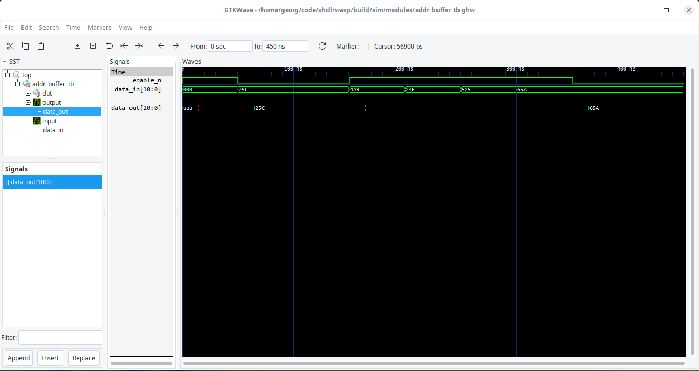
If the Enable signal is in high state, the output pins are in high-impedance state. Else, the output pins mirror the input pins. That’s a buffer.
Conclusion
I laid out some basics for taking the next design steps. Two of the three new modules have been implemented here. Next time, I’ll implement the missing Address Counter. This will be the first module of the Wasp that will deal with the clock too. So I’ll leave it for its own post. Once that is done, I’ll put them together to create the improved version of the Wasp.