Prelude
Last time, I wrote a simple control signal generator and address buffer for the Wasp. This post will explain how I derive a synchronous circuit for the control signal generator from a timing diagram. I’ll push the design of the address counter to the next post.
Here’s a basic overview of my design process. In this post, I want to improve the Control Signal Generator by adding an Examine switch. When the Examine switch is pressed, the Wasp will read the datum at the address selected with the input switches. The output LEDs will then be updated to display the new datum and address.
I’ll start by drawing up an “ideal” timing diagram. This timing diagram will show when which control signal will have to change to perform the Examine task. The timing diagram will also show the data changes on the data and address bus.
Next, I’ll turn that timing diagram into a finite-state machine, more precisely, a Moore machine. This will be an abstract representation of the control signal generator.
Finally, I will derive a synchronous digital circuit from this state machine that will generate the correct control signals.
A Timing Diagram for Accessing RAM
Here’s the timing diagram that shows all signals when RAM is accessed:
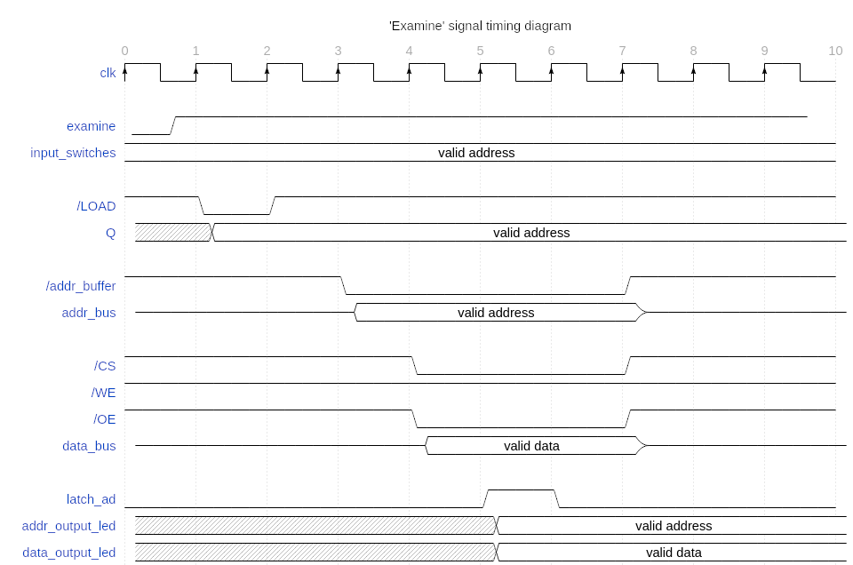
Let’s start at the top. The signals examine and input_switches represent the state of the front panel switches. For now, assume that examine is already debounced but asynchronous in regard to the clock (I will take care of the analog parts of the Wasp when I draw up the actual schematics).
When the examine switch is pressed, we first need to load the selected address onto the address bus. That’s what the address counter and buffer will do.
Next, /LOAD and Q (signal names prefixed with / denote active-low signals). These represent the control signal and counter output, respectively.
We send an (active low) signal /LOAD to preset the counter to our input value from input_switches. The counter’s output Q will then update to the new address. Then we tell the address buffer to change from a high-impedance state to active and latch the address provided by Q onto the address bus.
Finally, we use /CS and /OE to read data from the RAM, send a single pulse to the output modules with latch_ad.
The control signal generator, therefore, has one input, examine, and six output signals; /LOAD, /addr_buffer, /CS, /WE, /OE, and latch_ad.
Generating the State Diagram and Table
This is actually the hardest step of the whole process. Once you have a correct (and, possibly, complete) state diagram, the remaining steps are pretty trivial.
Since I’m designing a Moore machine, the six outputs will change whenever the state changes. States will change according to the one input signal, examine. Therefore, I need to find all the states this Moore machine can have. Let’s take the timing diagram from above and mark all times when one or more of the output signals change:
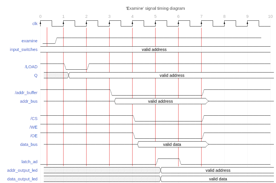
So, there is a total of eight states. Let’s give them names, starting left:
- idle: The standard or starting state. Whenever there is no button pressed, the machine is in idle state.
-
load_addr: Once the Examine switch is pressed, we first need to tell the address counter to latch the input. So
/LOADhas to change to low. -
stable_counter: The address to be examined is now latched into the address counter so we can put
/LOADback to high. -
buffer_addr: Next, we activate the address buffer, so
/addr_bufferhas to go low. -
select_ram: Now, that the correct address is on the address bus, we can activate the RAM chip by pulling both
/CSand/OEto low. -
update_output: We put the signal for the output modules
latch_adinto high to latch the new data and address to the output LEDs. -
output_updated: The outputs are updated so
latch_adcan be low again. -
wait: Finally, we deselect the RAM and put the address buffer back into high-impedance state by pulling
/addr_buffer,/CS, and/OEback to high state.
Let’s turn this timing diagram into a state diagram:
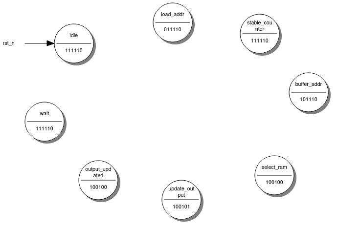
Here you can see all eight states. Below each state are the current values of each output we want the machine to produce. These values are taken directly from the timing diagram above. Next, we add the state transitions according to input. This is pretty simple since there is only one input signal, examine:
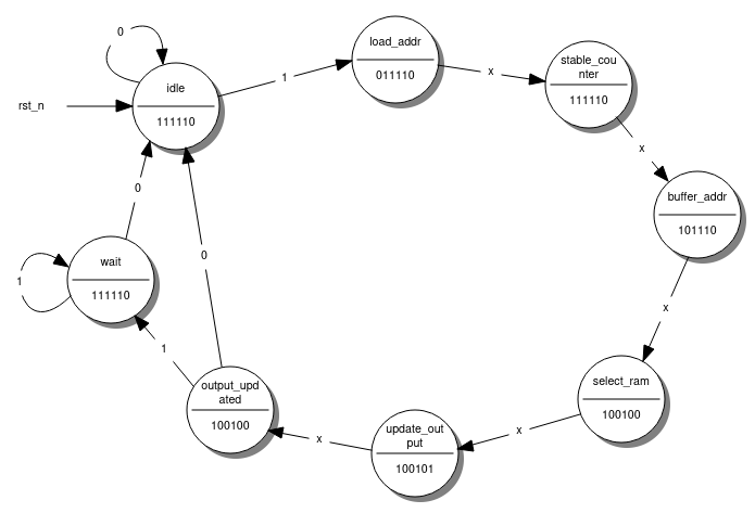
The machine starts in the idle state. As long as the input is low/zero (a.k.a., the Examine button is not pressed), nothing happens. When the input is high/one, the state changes to load_addr and runs through all the states, regardless of the input. The wait state is kind of a “re-trigger” protection; it waits until the Examine button is released again before returning to idle state.
Here’s a good point to note that the timing diagram above is just one possible solution for accessing RAM. This is highly dependent on the kind of memory and components you’re using. As I said, this is the hardest part of the process. You need to study your chips’ datasheets closely to understand how (and when) to generate the correct control signals.
It is also possible to optimize finite-state machines. But I’ll skip this step for simplicity (this state machine is simple enough to understand on its own). My goal here is to show how to turn a given timing diagram into a working digital circuit with the help of finite-state machines.
Now that we have an unambiguous and complete finite-state machine in the form of a state diagram, we need to translate it into a state transition table. I prefer one-dimensional state transition tables since it is easier to translate them into Boolean expressions for the next step. Here’s the state diagram where I assign every state a unique binary number.

Now, I simply list all possible state and input combinations and add which new state the machine should take on according to the current input.
I use A+, B+, and C+ to represent the next state we want the machine to transition to according to input:
| State Transition Table | ||||||||||||
|---|---|---|---|---|---|---|---|---|---|---|---|---|
| Current State | Input | Next State | Output | |||||||||
| A | B | C | A+ | B+ | C+ | |||||||
| 0 | 0 | 0 | 0 | 0 | 0 | 0 | 111110 | |||||
| 0 | 0 | 0 | 1 | 0 | 0 | 1 | ||||||
| 0 | 0 | 1 | 0 | 0 | 1 | 0 | 011110 | |||||
| 0 | 0 | 1 | 1 | 0 | 1 | 0 | ||||||
| 0 | 1 | 0 | 0 | 0 | 1 | 1 | 111110 | |||||
| 0 | 1 | 0 | 1 | 0 | 1 | 1 | ||||||
| 0 | 1 | 1 | 0 | 1 | 0 | 0 | 101110 | |||||
| 0 | 1 | 1 | 1 | 1 | 0 | 0 | ||||||
| 1 | 0 | 0 | 0 | 1 | 0 | 1 | 100100 | |||||
| 1 | 0 | 0 | 1 | 1 | 0 | 1 | ||||||
| 1 | 0 | 1 | 0 | 1 | 1 | 0 | 100101 | |||||
| 1 | 0 | 1 | 1 | 1 | 1 | 0 | ||||||
| 1 | 1 | 0 | 0 | 0 | 0 | 0 | 100100 | |||||
| 1 | 1 | 0 | 1 | 1 | 1 | 1 | ||||||
| 1 | 1 | 1 | 0 | 0 | 0 | 0 | 111110 | |||||
| 1 | 1 | 1 | 1 | 1 | 1 | 1 | ||||||
That’s all there is to the state diagram and table. Now I can create the circuit.
Translating a Finite State Machine to a Digital Circuit
The final step is almost trivial. I use the state table above to generate a circuit based on simple logic gates and flip-flops.
The finite-state machine has a total of 8 states, so I need some kind of component to keep track of that. This is done pretty simply with three D-type flip-flops. Each flip-flop can have two states, 0 or 1. So combining three flip-flops into some kind of 3-bit register is sufficient.
Next, I need to determine the input of each flip-flop. For this, we take the state table above. Each flip-flop represents one bit of the 3-bit state numbers. I name the MSB bit A, the middle one B, the LSB C.
To determine the input expression for the flip-flop A (called A+ in the state table above), I only need to use some established reduction method for Boolean expressions, like Karnaugh maps or, my preference, Quine-McCluskey method. I simply look at each column of the next state section and think of each as a four-input Boolean function and simplify it with the JQM tool:
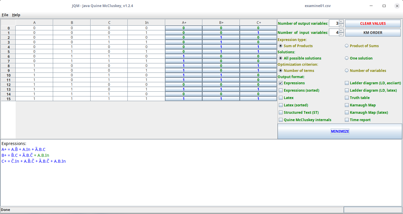
Using Quine-McCluskey these 4-input functions can be simplified to
Now rinse and repeat for each output signal, except that I only use the current state and output columns of the state transition table. Remember, this is a Moore machine so the output signals are only dependent on the current state. Here are all output signals as Boolean expressions:
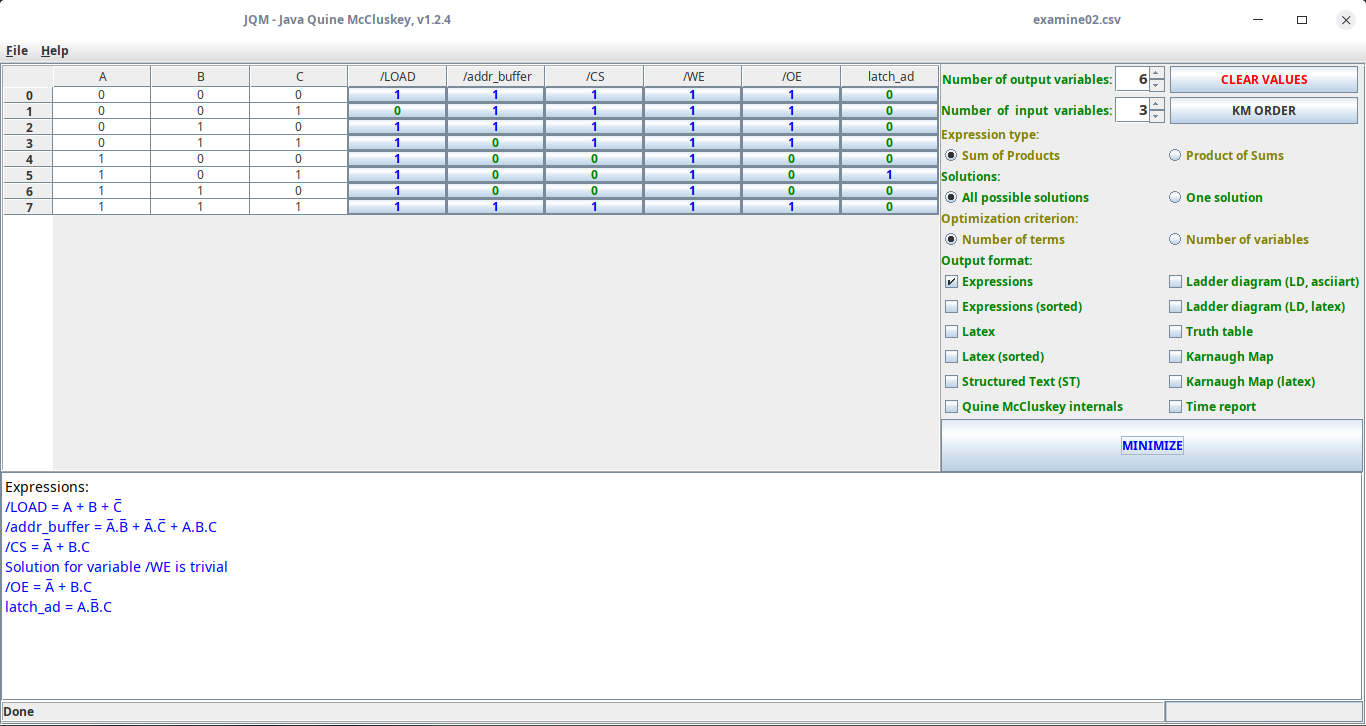
Using the Quine-McCluskey method again yields these results:
I created the circuit in this text file you can load into this circuit simulator to see it in action. Go to the File menu and Import From Text. The Examine switch is the one in the upper-left corner of the circuit it.
Here’s a schematic of this circuit:
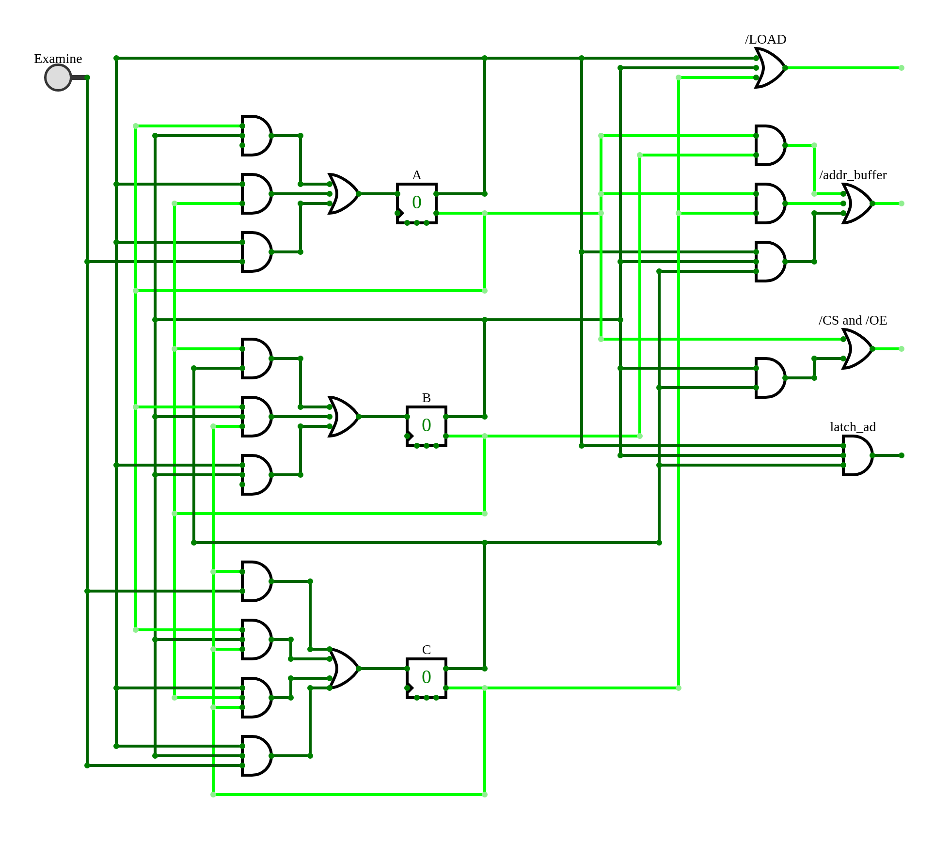
And that’s it. (NOTE: I forgot to add the clock in the schematic above; I’ll fix that as soon as I get back to a Windows machine with Altium on it.)
There are a few caveats. For one, as I said before, the state machine itself is not optimized, nor is the timing diagram it is based on. For example, you could merge the stable_counter and buffer_addr into one state.
Also, I used a mix of 2-, 3-, and 4-input gates in the schematic above. If you were to build this circuit from 74-series logic chips, you’d also need to adjust for propagation delay and structural hazards. You’d probably also split or merge certain signals to optimize for gate and/or chip count, respectively. There are some duplicate gates/signals in the circuit above, too.
I skipped those steps to showcase my design process: Create the timing diagram based on the chips’ datasheets, create the state diagram and table, translate it to a digital circuit. After all this, you’d go back to each step, look for errors and find ways to optimize the design.
Conclusion
This is how I turn a timing diagram into a digital circuit. Mind that this is in no way the only way to do it. I only had to juggle eight different states. Now imagine the state table for 16 states and four inputs, that’s a state table with 256 entries! Doing this “manually” as I did above would be quite work-intense.
But with the help of algorithms and methods like Quine-McCluskey that can be implemented as (relatively) simple programs and scripts, like JQM I used above. In a later post, I’ll show you how to use this approach to design a more complex signal generator that will handle a lot more input and output. This will also include methods of optimizing finite-state machines.
Next time, I’ll finally design the address counter using the method described here.